

Just a guy with a lot of silicon, a camera, and some spare time.
Joined April 2021
- Tweets153
- Following15
- Followers684
- Likes1.1K


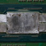




I swear, Intel must be paid by big solder. All their recent stuff I’ve touched has a gallon of solder between the IHS and the package. Messed up some of the power delivery too when the IHS finally popped… guess I’ll have to do some composite work once I get board photos done.


Well that wasn't what I ordered, I wanted PonteVecchio. Turns out some of the Arctic Sound HP tiled chips made it into engineering samples that got into the wild. Never thought I'd see one of these after they got memory holed.


For those of you who don't recall (because Intel deleted Architecture Day 2020 from their archives) here's an article about the cancelation that includes a few of the old slides: videocardz.com/newz/raja-kod…

I hadn't tried delidding a Skylake SP package until today. My god are these things awful. Like competing with IBM levels of obnoxious to get apart cleanly. I assumed it was one set of rubber sealant and solder, no! It's two separate layers on different PCBs at different heights!
3
947
Been a while. Last time I posted was just before I started the process of buying a house. I now have a much larger space I'm just about settled in, that means permanent sanding and photography areas so hopefully my output will increase in the near future.

Hello, not dead; been busy. Got a few more rarities for the collection. Still got SPR to finish up, we'll see how far I get with that. Would be nice to be fully done with that by EoY. Now I only need PVC, Arc, and CSL-AP to fill out most of Intel's recent massive flops.


1
10
561
Anyone have any helpful advice for where to start on this? I had a bad cap on -12V which got me to post, then I put my MDA back in hooked it up and got the first video as a result which was stable. Then tied with the floppy card and keyboard plugged in and got the second result.

Anyone know how to get rid of this horrific new underfill Intel uses without damaging components or the board?


I'm curious if anyone can identify this. I'll post what it is if nobody guesses in the next day or two.


