The AI-ready collaborative platform driving the #DigitalTransformation of #materials and #chemicals R&D through #modeling and #machinelearning.
San Francisco, CA
Joined November 2018
- Tweets1K
- Following475
- Followers3.7K
- Likes649
Pinned Tweet
Twitter
Welcome to the Era of Digitally-Engineered Mat3rials!
Thank you @WSJ + @newsient for sharing the news about our $3M seed round, solid growth + how our platform accelerates #RnD of #materials and #chemicals!
ow.ly/VprM50HMwJM
๐ฌ ๐ฅ๐ฒ๐น๐ฒ๐ฎ๐๐ฒ ๐๐ถ๐ด๐ต๐น๐ถ๐ด๐ต๐: ๐๐ฟ๐ฎ๐ฝ๐ต๐ฒ๐ป๐ฒ ๐ผ๐ป ๐ฆ๐๐ฏ๐๐๐ฟ๐ฎ๐๐ฒ๐
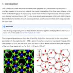
Release 2026.10.29 adds new examples that compute how a substrate changes the electronic structure of graphene.
A new tutorial builds graphene on O-terminated ฮฑ-quartz(0001) in the metastable geometry of Kang et al. (Phys. Rev. B, 2008). As in the publication, the graphene comes out p-doped, with the Dirac point 1.171 eV above the Fermi level against the published 1.28 eV.
A companion example places graphene on hexagonal boron nitride and calculates the stacking energy and the small band gap that the substrate opens at the Dirac point (Giovannetti et al., Phys. Rev. B, 2007).
Explore Release 2026.10.29: mat3ra.com/news-and-blog-posโฆ
๐ Try it for free at mat3ra.com/?utm_source=twittโฆ
#Mat3ra #Graphene #2DMaterials #DFT #BandStructure #MaterialsScience
1
109
โก ๐ ๐ฎ๐๐ฏ๐ฟ๐ฎ ๐ฎ๐ฑ๐ฑ๐ ๐ก๐ฉ๐๐๐๐ ๐๐๐๐๐๐ ๐ ๐ณ๐ผ๐ฟ ๐ฐ๐ฌโ๐ฒ๐ฌ๐
๐ณ๐ฎ๐๐๐ฒ๐ฟ ๐ฎ๐ป๐ฑ ๐ฒ๐ฎ๐๐ถ๐ฒ๐ฟ-๐๐ผ-๐ฑ๐ฒ๐ฝ๐น๐ผ๐ ๐บ๐ฎ๐๐ฒ๐ฟ๐ถ๐ฎ๐น๐ ๐๐ถ๐บ๐๐น๐ฎ๐๐ถ๐ผ๐ป๐
AI can propose new materials faster than anyone can test them. Mat3ra now helps clear that bottleneck with NVIDIA ALCHEMI.
๐ช๐ต๐ฎ๐'๐ ๐ป๐ฒ๐:
ยทยทยทยทยทยทยทยทยทยทยทยทยทยทยทยทยทยทยทยทยทยทยทยทยทยทยทยทยทยทยทยทยทยทยทยทยทยทยทยทยทยทยทยทยทยทยทยท
๐ One NVIDIA H100 NVL GPU relaxed 4,000 crystal structures in about 3 minutes, versus close to 3 hours one at a time
๐งฎ ALCHEMI Toolkit 0.3.0 simulates hundreds of structures at once on a single GPU, with results consistent with the one-at-a-time approach
๐ Run it from a notebook on the Mat3ra platform: no software to install, no GPU to buy, and you can plug in your own structures
ยทยทยทยทยทยทยทยทยทยทยทยทยทยทยทยทยทยทยทยทยทยทยทยทยทยทยทยทยทยทยทยทยทยทยทยทยทยทยทยทยทยทยทยทยทยทยทยท
Benchmark: strained, randomly displaced 64-atom cells, MACE-MPA-0 with cuEquivariance. Throughput varies with structures, model and hardware.
A guest post by Takuya Shibayama and Mitsunori Nakamoto (NVIDIA).
๐ Read the full story:
mat3ra.com/news-and-blog-posโฆ
#NVIDIA #ALCHEMI #MACE #GPU #MaterialsScience #Mat3ra
๐ ๐ฅ๐ฒ๐น๐ฒ๐ฎ๐๐ฒ ๐๐ถ๐ด๐ต๐น๐ถ๐ด๐ต๐: ๐๐ฎ๐ป๐ฑ ๐ข๐ณ๐ณ๐๐ฒ๐๐ ๐ฎ๐ ๐ฆ๐ฒ๐บ๐ถ๐ฐ๐ผ๐ป๐ฑ๐๐ฐ๐๐ผ๐ฟ ๐๐ป๐๐ฒ๐ฟ๐ณ๐ฎ๐ฐ๐ฒ๐
Release 2026.10.29 adds two new examples that calculate the valence band offset at a semiconductor heterojunction with the platform's valence band offset workflow.
Each one builds a strained superlattice and the matching bulk references, then lines up the bulk valence band maxima through the average electrostatic potential across the interface:
โช๏ธ Si/Ge (001), following Van de Walle and Martin (Phys. Rev. B, 1986): 0.765 eV, against 0.74 eV in the publication
โช๏ธ GaAs/AlAs (110), following Hinuma et al. (Phys. Rev. B, 2014): 0.471 eV, against the published 0.45 eV
Explore Release 2026.10.29: mat3ra.com/news-and-blog-posโฆ
๐ Try it for free at mat3ra.com/?utm_source=twittโฆ
#Mat3ra #BandOffset #Semiconductors #DFT #Heterojunction #MaterialsScience
โ๏ธ Mat3rials 3xplorer.
๐๐ป๐๐ฒ๐ฟ๐ณ๐ฎ๐ฐ๐ฒ ๐ฏ๐ฒ๐๐๐ฒ๐ฒ๐ป ๐๐ฎ๐น๐น๐ถ๐๐บ ๐ก๐ถ๐๐ฟ๐ถ๐ฑ๐ฒ ๐ฎ๐ป๐ฑ ๐๐น๐๐บ๐ถ๐ป๐๐บ ๐ข๐
๐ถ๐ฑ๐ฒ (๐๐ฎ๐ก(๐ฌ๐ฌ๐ญ)/๐๐น๐ฎ๐ข๐ฏ(๐ฌ๐ฌ๐ญ)), ๐๐๐ฟ๐ฎ๐ถ๐ป-๐บ๐ฎ๐๐ฐ๐ต๐ถ๐ป๐ด ๐๐๐ฝ๐ฒ๐ฟ๐ฐ๐ฒ๐น๐น.
Available online in our materials bank:
platform.mat3ra.com/bank/matโฆ
#mat3rials3xplorer #materialsscience #mat3ra #Semiconductors #GaN
3
6
136
๐ ๐ฅ๐ฒ๐น๐ฒ๐ฎ๐๐ฒ ๐๐ถ๐ด๐ต๐น๐ถ๐ด๐ต๐: ๐ฆ๐ฐ๐ต๐ผ๐๐๐ธ๐ ๐๐ฎ๐ฟ๐ฟ๐ถ๐ฒ๐ฟ ๐๐ฒ๐ถ๐ด๐ต๐
Release 2026.10.29 adds a new Quantum ESPRESSO workflow that calculates the Schottky barrier height at a metal/semiconductor contact.
It shares the electrostatic potential steps with the band offset workflow and lines up the metal Fermi level with the semiconductor band edges through the averaged potential across the interface. The job page reports the p-type and n-type barrier heights as separate results.
Explore Release 2026.10.29: mat3ra.com/news-and-blog-posโฆ
๐ Try it for free at mat3ra.com/?utm_source=twittโฆ
#Mat3ra #SchottkyBarrier #Semiconductors #DFT #QuantumESPRESSO #MaterialsScience
5
8
208
๐ ๐ ๐ฒ๐ฒ๐ ๐ค๐๐ฎ๐ป๐๐๐บ ๐ฏ๐
๐ฝ๐น๐ผ๐ฟ๐ฒ๐ฟ (๐ค๐ฏ): ๐ฎ๐ป ๐๐-๐ป๐ฎ๐๐ถ๐๐ฒ ๐ฒ๐ป๐ด๐ถ๐ป๐ฒ ๐ณ๐ผ๐ฟ ๐พ๐๐ฎ๐ป๐๐๐บ ๐บ๐ฎ๐๐ฒ๐ฟ๐ถ๐ฎ๐น๐ ๐บ๐ผ๐ฑ๐ฒ๐น๐ถ๐ป๐ด
A quantum simulation engine written from scratch by AI agents, under the direction and supervision of domain scientists. Developed in weeks rather than years, and open source (Apache 2.0) as part of CAMSAI.org.
What Q3 does:
โ๏ธ Plane-wave pseudopotential DFT: norm-conserving, ultrasoft and PAW, with spin polarization, Hubbard U, dispersion corrections, forces, stresses and structural relaxation
โ
Reproduces established reference implementations and runs faster on a single core in representative benchmarks
๐ฅ๏ธ Scales across GPU-accelerated supercomputers
๐ Runs unmodified Quantum ESPRESSO pw.x inputs and reads UPF pseudopotentials
Mat3ra is part of the team behind the effort, with co-authors from Berkeley Lab/NERSC, UC Berkeley, Stanford, SLAC, USC, Johns Hopkins, AFRL and NVIDIA.
๐ Read more:
mat3ra.com/news-and-blog-posโฆ
๐ Preprint: arxiv.org/abs/2610.42108
๐ป Code: github.com/camsai/q3
#Mat3ra #Quantum3xplorer #CAMSAI #DFT #OpenSource #AIforScience #MaterialsScience
3
4
333
๐ ๐ ๐ฎ๐๐ฏ๐ฟ๐ฎ ๐ฃ๐น๐ฎ๐๐ณ๐ผ๐ฟ๐บ ๐ฅ๐ฒ๐น๐ฒ๐ฎ๐๐ฒ ๐ฎ๐ฌ๐ฎ๐ฒ.๐ญ๐ฌ.๐ฎ๐ต
Our latest platform release introduces new capabilities for computational materials research.
Key additions include:
โช๏ธ New workflow: Schottky barrier height at metal/semiconductor contacts
โช๏ธ Valence band offsets for Si/Ge and GaAs/AlAs interfaces
โช๏ธ Graphene on substrates, including p-doping on ฮฑ-quartz
โช๏ธ Point defects in graphene and GaN
โช๏ธ More examples that reproduce published results: SrTiOโ(011) surface energies and a Ptโ cluster on monolayer MoSโ
The release also includes interface improvements, bug fixes, and updates for developers.
๐ Also new: our paper "AI-ready design of realistic 2D materials and interfaces with Mat3ra-2D"
nature.com/articles/s41598-0โฆ
Explore the complete release: mat3ra.com/news-and-blog-posโฆ
๐ Try it for free at mat3ra.com/?utm_source=twittโฆ
#Mat3ra #PlatformRelease #MaterialsScience #ComputationalMaterials #DFT #Semiconductors #Graphene
6
7
158
โกNewsletter 2026/10. Platform Release and News! - mailchi.mp/a9157684b883/joinโฆ
2
143
โ๏ธ Mat3rials 3xplorer.
๐๐ถ๐๐๐ผ๐ฐ๐ถ๐ฎ๐๐ถ๐๐ฒ ๐ฎ๐ฑ๐๐ผ๐ฟ๐ฝ๐๐ถ๐ผ๐ป ๐ผ๐ณ ๐ข๐
๐๐ด๐ฒ๐ป ๐ผ๐ป ๐ฎ ๐ฃ๐น๐ฎ๐๐ถ๐ป๐๐บ (๐ญ๐ญ๐ญ) ๐๐๐ฟ๐ณ๐ฎ๐ฐ๐ฒ (๐ฃ๐(๐ญ๐ญ๐ญ)โ๐ฎ๐ข), ๐ฟ๐ฒ๐น๐ฎ๐
๐ฒ๐ฑ ๐ฏร๐ฏร๐ญ ๐๐น๐ฎ๐ฏ ๐๐๐ฝ๐ฒ๐ฟ๐ฐ๐ฒ๐น๐น.
Available online in our materials bank:
platform.mat3ra.com/bank/matโฆ
#mat3rials3xplorer #materialsscience #mat3ra #Catalysis #SurfaceScience
3
5
184
โกNewsletter 2026/10. Platform Release and News! - mailchi.mp/e22b1d38d13e/joinโฆ
141
๐ ๐ก๐ผ๐ ๐ฎ๐๐ฎ๐ถ๐น๐ฎ๐ฏ๐น๐ฒ ๐ผ๐ป ๐ก๐ฎ๐๐๐ฟ๐ฒ.๐ฐ๐ผ๐บ: ๐๐-๐ฟ๐ฒ๐ฎ๐ฑ๐ ๐ฑ๐ฒ๐๐ถ๐ด๐ป ๐ผ๐ณ ๐ฟ๐ฒ๐ฎ๐น๐ถ๐๐๐ถ๐ฐ ๐ฎ๐ ๐บ๐ฎ๐๐ฒ๐ฟ๐ถ๐ฎ๐น๐ ๐๐ถ๐๐ต ๐ ๐ฎ๐๐ฏ๐ฟ๐ฎ-๐ฎ๐
AI/ML models for materials are mostly trained on ideal bulk crystals, while real devices are dominated by surfaces, interfaces and defects. Realistic structures have to be built and documented, not just picked from a database.
Mat3ra-2D is our open-source framework for generating realistic 2D materials, slabs, interfaces, defects and disorder.
What's inside:
๐งฑ Define โ Refine โ Build workflows: every structure keeps its provenance, including the source materials and build parameters (Miller indices, layers, vacuum, termination, strain, shift)
๐ 23 reusable notebooks that run in any browser, no installation: jupyterlite.mat3ra.com
๐ฆ Representative structures in the public Materials Explorer (platform.mat3ra.com), archived on Figshare: doi.org/10.6084/m9.figshare.โฆ
๐ Open source, interoperable with pymatgen and ASE
It is the structure-generation layer that comes before property calculations and ML training.
Authors: Vsevolod Biryukov, Kamal Choudhary (Johns Hopkins University) and Timur Bazhirov. Supported in part by NIST. Open access.
๐ Read the paper:
nature.com/articles/s41598-0โฆ
#MaterialsScience #OpenScience #AIforScience #Mat3ra
2
221
๐ ๐ ๐ฎ๐๐ฒ๐ฟ๐ถ๐ฎ๐น ๐ผ๐ณ ๐๐ต๐ฒ ๐ ๐ผ๐ป๐๐ต: ๐๐ฎ๐๐(๐ฌ๐ฌ๐ญ)/๐๐น๐๐(๐ฌ๐ฌ๐ญ) ๐๐ป๐๐ฒ๐ฟ๐ณ๐ฎ๐ฐ๐ฒ
This model represents a strain-matched interface between two closely lattice-matched III-V semiconductors, combining the GaAs(001) and AlAs(001) surfaces in a single supercell. GaAs/AlAs heterostructures are a foundational system in semiconductor physics, long used to study band alignment, quantum confinement, and superlattice behavior at the atomic scale.
The GaAs(001)/AlAs(001) system can be used to explore structureโproperty relationships in III-V semiconductor heterostructures and to study how atomic-scale interface configurations influence electronic and optoelectronic device behavior โ relevant to applications such as high-electron-mobility transistors (HEMTs), quantum-well lasers, and distributed Bragg reflectors.
Explore this featured GaAs/AlAs interface model on the Mat3ra platform:
platform.mat3ra.com/bank/matโฆ
#MaterialOfTheMonth #Semiconductors #GaAs #IIIV #MaterialsScience #Mat3ra
4
8
273
โ๏ธ Mat3rials 3xplorer.
๐๐ป๐๐ฒ๐ฟ๐ณ๐ฎ๐ฐ๐ฒ ๐ฏ๐ฒ๐๐๐ฒ๐ฒ๐ป ๐ง๐ถ๐๐ฎ๐ป๐ถ๐๐บ ๐ก๐ถ๐๐ฟ๐ถ๐ฑ๐ฒ ๐ฎ๐ป๐ฑ ๐ฆ๐ถ๐น๐ถ๐ฐ๐ผ๐ป (๐ง๐ถ๐ก(๐ฌ๐ฌ๐ญ)/๐ฆ๐ถ(๐ฌ๐ฌ๐ญ)), ๐๐๐ฟ๐ฎ๐ถ๐ป-๐บ๐ฎ๐๐ฐ๐ต๐ถ๐ป๐ด ๐๐๐ฝ๐ฒ๐ฟ๐ฐ๐ฒ๐น๐น.
Available online in our materials bank:
platform.mat3ra.com/bank/matโฆ
#mat3rials3xplorer #materialsscience #mat3ra #Semiconductors #DFT
3
197
๐ ๐ ๐ฎ๐๐ฏ๐ฟ๐ฎ ๐ฎ๐ ๐๐ต๐ฒ ๐๐ฒ๐ป๐ฒ๐๐ถ๐ ๐ ๐ถ๐๐๐ถ๐ผ๐ป ๐๐ฎ๐ฐ๐ธ๐ฎ๐๐ต๐ผ๐ป, ๐ฎ๐น๐ผ๐ป๐ด๐๐ถ๐ฑ๐ฒ ๐๐ผ๐ผ๐ด๐น๐ฒ, ๐๐ช๐ฆ ๐ฎ๐ป๐ฑ ๐ข๐ฝ๐ฒ๐ป๐๐
Three days. One national lab. Some of the biggest names in tech, all working on one goal: AI that accelerates science.
From October 14 to 16, Argonne National Laboratory hosted the Genesis Mission Hackathon, and Mat3ra took part as an Industrial Partner, alongside Google, AWS, Microsoft, OpenAI and IBM Research.
What made it exciting:
โ๏ธ Genesis Mission teams worked with technical experts to bring their scientific workflows onto the DOE Genesis Mission Platform
๐งช Materials discovery is one of the places where this pays off, and we have three selected Genesis Mission projects, including AlphaFilm for thin film discovery
๐ค Our Founder and CEO, Timur Bazhirov, represented Mat3ra in the room
AI, data and computing are coming together to speed up science, and Mat3ra is right in the middle of it.
๐ Read the full story:
mat3ra.com/news-and-blog-posโฆ
#GenesisMission #DOE #MaterialsScience #AIforScience #Mat3ra
3
4
270
๐ ๐ช๐ฒ'๐ฟ๐ฒ ๐๐ถ๐ฟ๐ถ๐ป๐ด ๐ฎ๐ ๐ ๐ฎ๐๐ฏ๐ฟ๐ฎ
Let's make Iron Man's Digital Materials R&D experience a reality together.
โ๏ธ Computational Materials Scientist
apply.workable.com/mat3ra/j/โฆ
Bridge materials/chemistry, data science, and computer science: apply nanoscale modeling across large sets of materials, surfaces, and reaction pathways; organize simulation and experimental data; build AI approaches on top of it.
๐งโ๐คโ๐ง Community Evangelist
apply.workable.com/mat3ra/j/โฆ
For outgoing scientists/engineers who want to grow a vibrant global community: identify pathways for community growth, prepare case studies and technical content, deliver it, and measure KPIs.
All open positions: apply.workable.com/mat3ra/
#Mat3ra #Hiring #JobOpenings #MaterialsScience #ComputationalMaterials
5
5
274
๐ฌ ๐จ๐ฝ๐ฐ๐ผ๐บ๐ถ๐ป๐ด ๐ช๐ฒ๐ฏ๐ถ๐ป๐ฎ๐ฟ: ๐๐น๐ฒ๐ฐ๐๐ฟ๐ผ๐ป๐ถ๐ฐ๐ โ ๐๐ฎ๐ป๐ฑ ๐ข๐ณ๐ณ๐๐ฒ๐ + ๐ฆ๐ฐ๐ต๐ผ๐๐๐ธ๐ ๐๐ฎ๐ฟ๐ฟ๐ถ๐ฒ๐ฟ
Join us October 28 for Mat3ra 2D, Season 2, Episode VII: Electronics โ Band Offset + Schottky Barrier.
This session demonstrates how to compute electronic interface properties โ band offset and Schottky barrier โ using Quantum ESPRESSO from JupyterLab notebooks on the Mat3ra platform. We'll cover practical workflows for obtaining and interpreting band alignment and carrier-injection barriers from atomistic simulations, with examples including HfOโ(001)/Si(001) and MoSโ/Au(111) interfaces.
Presenter: Vsevolod (Seth) Biryukov, Scientific Software Engineer
Host: Timur Bazhirov
Language: English
๐๏ธ October 28, 2026 โ 07:30 PDT / 10:30 EDT / 14:30 GMT / 15:30 CET / 16:30 EET / 20:00 India / 22:30 Singapore / 23:30 Japan
๐ Online via Zoom
Register to attend: mat3ra.com/events-posts/mat3โฆ
#Mat3ra #Webinar #MaterialsScience #DFT #QuantumESPRESSO #Semiconductors
๐ ๐ฅ๐ฒ๐๐ฒ๐ฎ๐ฟ๐ฐ๐ต ๐ช๐ฒ ๐๐ผ๐๐ฒ: ๐๐น๐ฒ๐ฐ๐๐ฟ๐ผ๐ป ๐๐บ๐ฎ๐ด๐ถ๐ป๐ด ๐ถ๐ป ๐ฆ๐ฒ๐บ๐ถ๐ฐ๐ผ๐ป๐ฑ๐๐ฐ๐๐ผ๐ฟ๐ & ๐๐ถ๐๐ฐ๐ผ๐๐ฒ๐ฟ๐ ๐๐ผ๐ผ๐ฝ
๐ ๐ก๐ฒ๐ ๐๐น๐ผ๐๐ฒ-๐จ๐ฝ ๐ฉ๐ถ๐ฒ๐ ๐ผ๐ณ ๐๐น๐ฒ๐ฐ๐๐ฟ๐ผ๐ป๐ ๐๐ป๐๐ถ๐ฑ๐ฒ ๐ฆ๐ฒ๐บ๐ถ๐ฐ๐ผ๐ป๐ฑ๐๐ฐ๐๐ผ๐ฟ๐
Berkeley Lab combined atomic-scale imaging (scanning tunneling microscopy) with Quantum Monte Carlo simulations to directly observe how electrons interact with defects in 2D semiconductors like molybdenum diselenide โ some defects act like "potholes," others like "speed bumps," as electrons shift between an ordered Wigner solid and a disordered Fermi liquid state. Published in Nature.
Authors: Mike Crommie, Feng Wang, et al. (UC Berkeley / Berkeley Lab, with Flatiron Institute, UC, University of New Mexico, Hofstra University, Arizona State University, and NIMS Japan)
๐ Source: newscenter.lbl.gov/2026/09/1โฆ
โโโโโโโโ โข โโโโโโโโ
๐๐ป๐๐ฟ๐ผ๐ฑ๐๐ฐ๐ถ๐ป๐ด ๐๐ถ๐๐ฐ๐ผ๐๐ฒ๐ฟ๐ ๐๐ผ๐ผ๐ฝ
A new AI startup founded by four Google AI veterans โ Jeff Dean, Sanjay Ghemawat, Quoc Le, and Oriol Vinyals โ aiming to automate the experimental loop of scientific and engineering research, running thousands of experiments in parallel with frontier AI models and compute infrastructure.
Authors: Jeff Dean, Sanjay Ghemawat, Quoc Le, Oriol Vinyals
๐ Source: discoveryloop.com/
#AIforScience #MaterialsScience #Semiconductors #Research
1
1
207
โ๏ธ Mat3rials 3xplorer.
๐๐ป๐๐ฒ๐ฟ๐ณ๐ฎ๐ฐ๐ฒ ๐ฏ๐ฒ๐๐๐ฒ๐ฒ๐ป ๐ฆ๐ถ๐น๐ถ๐ฐ๐ผ๐ป ๐๐ฎ๐ฟ๐ฏ๐ถ๐ฑ๐ฒ ๐ฎ๐ป๐ฑ ๐๐ฎ๐น๐น๐ถ๐๐บ ๐ก๐ถ๐๐ฟ๐ถ๐ฑ๐ฒ (๐ฆ๐ถ๐(๐ฌ๐ฌ๐ญ)/๐๐ฎ๐ก(๐ฌ๐ฌ๐ญ)), ๐๐๐ฟ๐ฎ๐ถ๐ป-๐บ๐ฎ๐๐ฐ๐ต๐ถ๐ป๐ด ๐๐๐ฝ๐ฒ๐ฟ๐ฐ๐ฒ๐น๐น.
Available online in our materials bank:
platform.mat3ra.com/bank/matโฆ
#mat3rials3xplorer #materialsscience #mat3ra #Semiconductors #DFT
1
6
158
๐๏ธUpcoming Webinar on Band Offset and Schottky Barrier, October 28th, Tokyo Materials Cafe, and AI 2 Science Happy Hour - mailchi.mp/02363a4ded8d/joinโฆ
1
163